Correlative Materials Characterization Workshop 2024
The goal of the workshop is to bring together communities from Materials, Life and Computer Science, to discuss and explore topics of common interests.
The scope of the event includes all relevant techniques used for correlative materials characterization. The main focus will be on Light Microscopy, Electron Microscopy, X-ray Microscopy and Atomic Force Microscopy.
Attendees expected: 80-100 (scientists, researchers, companies, practitioners and participants of the European School for Young Materials Scientists (a satellite event organised in Dresden on 4-5 November)).
Scientific Committee: Andre Clausner (Fraunhofer IKTS, Germany), Tomas Sikola (TU Brno/CEITEC, Czech Republic), Pavel Tomancak (CEITEC, Czech Republic), Ehrenfried Zschech (BTU Cottbus, Germany), Jan Neuman (NenoVision, Brnoregion Microscopy, Czech Republic)
Organisers: Fraunhofer IKTS, GlobalFoundries, Czech Optical Cluster, CEITEC, NenoVision
Participation fee: free of charge, registration required
CMC 2024 Workshop Program
Date: November 6 and 7, 2024
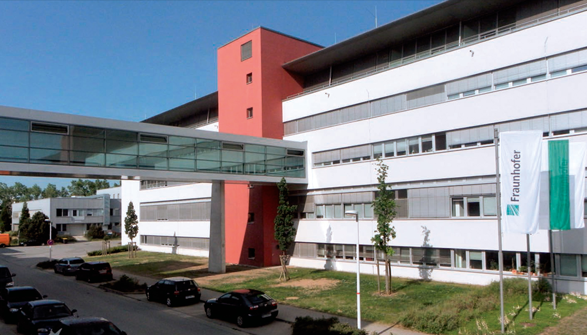
Location: Fraunhofer IKTS, Maria‐Reiche‐Strasse 2, 01109 Dresden, Germany
Room: Fraunhofer, 4th floor
Wednesday, November 6, 2024
- 11:30 Registration
- 12:30 Welcome by the Organizers
- André Clausner, Fraunhofer IKTS
- Silicon Saxony
- Czech Optical Cluster
- 13:00 Correlative in-situ and on-surface Analysis
- Observing while it happens: operando electron microscopy of non-equilibrium dynamics (Marc Willinger, TU Munich)
- Correlative scanning probe and luminescence microscopy to image structural obstacles for charge carriers (Ilka Hermes, Leibniz Institute for Polymer Research)
- Industry talk Bruker Nano
- AFM in-situ SEM studies of organic and inorganic materials (Ifat Kaplan-Ashiri, Weizmann Institute of Science)
- Industry talk NenoVision
- Next-Gen Batteries: understanding storage mechanisms and degradation phenomena (Holger Althus, Fraunhofer IWS)
- 14:40 Coffee Break
- 15:10 Correlative Analysis in Semiconductor Failure Analysis
- Synchronized multi-channel multi-technique characterization in SEM and STEM (René Hammer, point electronic GmbH)
- Industry talk IMINA
- Advanced In-Situ Analysis with AFM-in-SEM: Enhancing Semiconductor Failure Analysis (Jan Neuman, NenoVision)
- Industry talk point electronics
- Complex materials analysis in high-volume semiconductor manufacturing - case studies (Andreas Meyer, Global Foundries)
- Industry talk ThermoFisher
- Correlative failure analysis flows at Infineon (Eckhard Langer, Infineon)
- 17:00 Postersession
- 17:50 Individual Transfer to Conference Dinner
- 19:00 Conference Dinner at Watzke am Goldenen Reiter
Thursday, November 7, 2024
- 9:00 Correlative Tomography and cryo-EM
- TBA (Yael Politi, TU Dresden)
- Multiscale XCT based Characterization and modelling of composite materials (Robert Filipek, AGH Krakow)
- Industry talk Infineon
- Industry talk Global Foundries
- Advanced Scale-Bridging Multi-Modal Analytics for Device and Material Optimization through Data Correlation and Machine Learning (Silke Christiansen, Fraunhofer IKTS)
- High-Resolution Imaging of Transient RNA Polymerase II Biomolecular Condensates (Richard Štefl, CEITEC)
- 10:40 Coffee Break
- 11:00 Multiscale and multimodal correlative Analysis
- Multimode Fiber-Based Holographic Endomicroscopy: A Hair-Thin Path to Deep Brain Imaging in Animal Models (Hanka Uhlirova, ISI CAS)
- The role of lattice distortions in coccoliths morphogenesis (Igor Zlotnikov, TU Dresden)
- Industry talk ZEISS
- At the Bridge between Biology and Material - Nanomaterial Application and Safety (Jörg Opitz, Fraunhofer IKTS)
- Industry talk TESCAN
- TBA (Malgorzata Kopycinska-Müller, Fraunhofer IKTS)
- 12:20 Closing Remarks
- 12:30 End
Sponsors and Partners
Speakers
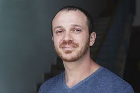
Igor Zlotnikov
TU Dresden, B Cube
Group Leader "Multiscale Analysis”
Title
The role of lattice distortions in coccoliths morphogenesis
Abstract
Coccoliths—micrometer-sized calcitic scales formed by unicellular algae are a prime example of biological regulation over crystal morphogenesis. Whereas calcite is expected to grow as a perfect rhombohedral crystal, coccolithophores are able to break the thermodynamically induced symmetry and morph calcite single-crystals into the most intricate shapes. Here, state-of-the-art X-ray-based coherent diffraction analysis and imaging methods were used to characterize local lattice properties in single calcitic units in coccoliths in 3D with a spatial resolution of 10 nm.
Bio
Dr. Igor Zlotnikov received his PhD in Materials Science and Engineering from Technion – Israel Institute of Technology. He then worked as a Postdoctoral Fellow and, subsequently, as a Researcher at the Max Planck Institute of Colloids and Interfaces. Currently, he is leading the group “Multiscale Analysis” in BCUBE – Center for Molecular Bioengineering, TU Dresden. His research focuses on the fundamental question of how nature takes advantage of thermodynamic principles to generate complex mineralized morphologies.
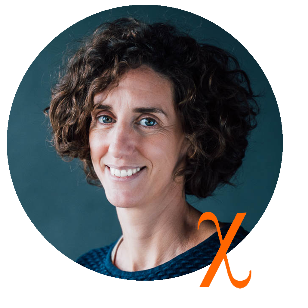
Yael Politi
TU Dresden, B CubeGroup Leader "Chitin-based Biological Materials and Biomineralization”
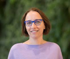
Ifat Kaplan-Ashiri
Weizmann Institute of Science
Staff Scientist at Department of Chemical Research Support
Title
AFM in-situ SEM studies of organic and inorganic materials
Abstract
I. Kaplan-Ashiri*, I. Rosenhek-Goldian, XM. Sui, N. Kampf and S. R. Cohen
Department of Chemical Research Support, Weizmann Institute of Science, 234 Herzl Street, Rehovot, Israel
AFM in-situ SEM is a valuable tool for materials’ characterization as it enables advanced imaging and spectroscopy with the various AFM and SEM modes. Preliminary AFM in-situ SEM imaging results of newly synthesized organic and inorganic materials will be presented. Morphological and topographical information gathered from SEM and AFM analyses were obtained from micro- and nanoscale particles, facilitating a deeper understanding of growth mechanisms and material properties.
Bio
Ifat Kaplan-Ashiri is an associate staff scientist at the Department of Chemical Research Support at the Weizmann Institute of Science (WIS) in Israel. She received her PhD in chemistry from WIS and had postdoc position in the University of Texas at Austin. Ifat joined the electron microscopy unit at WIS on 2012, and she is heading the SEM team. Her main fields of interest are imaging and spectroscopy of new and ancient materials as well as method development of spectroscopies (EDS and CL) in cryo-SEM for life science and in-situ and correlative SEM techniques.

Jan Neuman
NenoVision
Jan Neuman, CEO and Co-founder
Title
Advanced In-Situ Analysis with AFM-in-SEM: Enhancing Semiconductor Failure Analysis
Abstract
The correlative in-situ AFM-in-SEM technique combines the strengths of both instruments, allowing precise, localized sample analysis without transferring samples between setups. I will showcase semiconductor case studies, highlighting novel approaches in failure analysis, conductivity mapping, and dopant characterization. The AFM-in-SEM approach enhances accuracy, streamlines workflows, and offers insights into complex systems, making it a valuable tool for semiconductor reliability and battery research.
Bio
Jan Neuman is the CEO and Co-founder of the NenoVision company, founded in 2015 as the spin-off of CEITEC (Central European Institute of Technology) in Brno, Czech Republic. He earned his Ph.D. in Physical and Materials Engineering at Brno University of Technology in the Czech Republic, focusing on the fabrication and characterization of nanostructures. He became fascinated by correlative microscopy, enabling a better understanding of the different aspects and properties of various materials at the nanoscale. His passion resulted in the commercialization of AFM-in-SEM solutions in NenoVision, enabling him to continue developing in-situ correlative microscopy technology.
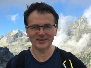
Robert Filipek
AGH Krakow
Full professor at Department of Physical Chemistry and Modelling
Title
Multiscale XCT based Characterization and modelling of composite materials
Abstract
Even up-to-date advanced studies of the transport processes and reactions in porous materials are described either by essentially homogeneous treatment of the system characterized by average volume parameters (e.g., porosity, permeability, tortuosity) or by a more sophisticated treatment of the system (including its real micro-structures), but with a simple transport model. Two examples will illustrate a new more general attempt for the description of transport and reactions in porous systems.
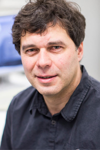
Eckhard Langer
Infineon Technologies
Director Physical Failure Analysis
Title
Correlative failure analysis flows at Infineon
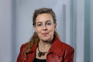
Silke Christiansen
Fraunhofer IKTS
Head of department: Correlative Microscopy and Materials Data
Title
Advanced Scale-Bridging Multi-Modal Analytics for Device and Material Optimization through Data Correlation and Machine Learning
Abstract
In the rapidly evolving fields such as electronics, battery technology and material science more in general, cutting-edge analytical approaches are essential to ensure device optimization, performance enhancement, and long-term reliability. Utilizing state-of-the-art tools such as x-ray microscopy (XRM), electron-ion microscopy (FIB-SEM), and Raman and infrared spectroscopies, we achieve a detailed correlative analysis. These methodologies are supported by nanoGPS technology, enabling precise multi-modal data correlation, which is critical in identifying imperfections and enhancing device performance. ncorporating advanced data analytics via machine learning algorithms within a proprietary platform, ‚XamFlow‘, adapted to our needs, we process and correlate extensive datasets, paving the way for predictive modeling in material and device optimization.
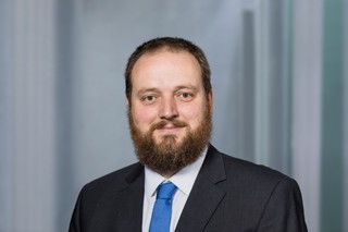
Jörg Opitz
Fraunhofer IKTS
Head of department: Bio- and Nanotechnology
Title
At the Bridge between Biology and Material - Nanomaterial Application and Safety
Abstract
Nanomaterials are transforming industries, but their safety is critical. This talk explores trends in nanomaterial regulation, focusing on biological systems and the unique challenges in measurement. By highlighting recent advances in synthesis and functionalization, we’ll discuss how nanomaterials, like nanodiamonds, can be safely integrated into biomedical applications.
Bio
Scientific Career
- Various positions at Fraunhofer Institutes, Dresden, Germany
- Since 04/2015: Head of Department ‘Bio- and Nanotechnology’ and Director of Business Unit ‘Bio- and Medical Technology’
- 2012 - 2015: Division Director ‘Condition Monitoring & Diagnostics’
- 2010 - 2012: Business Unit Manager ‘Environmental Technology and Energy Technology, Life Science’
- 2007 - 2008: Scientific Staff and Deputy Head of Department ‘Optical Diagnosis’ and Head of Group ‘Nanotechnology and Optical Sensors’
- Since 2009: Lecturer at BIOTEC and Max-Bergmann-Center of Biomaterials
- 2013 - 2015: Head of Group ‘Biocompatibility of Electronics Packaging’ (Electronics Packaging Laboratory)
- 2010 - 2014: Head of Group ‘InnovaSens’ (Max-Bergmann-Center of Biomaterials)
Scientific Focus: BioNanotechnology, Nanoparticle, Sensor Technology, Medical Application, Solid State Physics
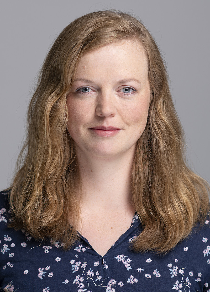
Ilka Hermes
Leibniz Institute for Polymer Research Dresden
Group Leader Correlative Atomic Force Microscopy
Title
Correlative scanning probe and luminescence microscopy to image structural obstacles for charge carriers
Abstract
With the miniaturization of (opto)electronic semiconductor devices, structural defects like grain or domain boundaries as well as strain-induced defects have an increased impact on the charge carrier transport. Here, electrical scanning probe microscopy allows capturing charge carrier accumulations, dopants and variations in the transport behavior. By complimenting SPM with luminescence detection, we are moreover able to visualize the impact of defects on ambipolar and excitonic transport.
Bio
Ilka Hermes studied chemistry at the Johannes Gutenberg University in Mainz. For her dissertation, she joined the Max Planck Institute for Polymer Research, where she used electrical and electromechanical SPM in combination with luminescence microscopy to study the impact of structural interfaces on charge carriers in perovskite solar cells. After three years in industry, Ilka started a junior research group for correlative SPM at the Leibniz Institute of Polymer Research in Dresden in 2022.
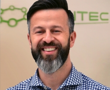
Richard Štefl
CEITEC MU
Group leader
Title
High-Resolution Imaging of Transient RNA Polymerase II Biomolecular Condensates
Abstract
Biomolecular condensates, which assemble in cells to regulate key biological processes, are challenging to study due to their inherently dynamic nature. In this talk, we will present our integrative multi-scale approach, which integrates light microscopy, electron cryomicroscopy, cryotomography, and coarse-grained simulations. Together, these methods reveal new insights into the molecular organization and biogenesis of a model RNA polymerase II condensate, shedding light on its structural complexity.
Bio
Richard Stefl is a structural biologist at the Central European Institute of Technology, specializing in RNA-protein interactions and biomolecular condensates. His research integrates advanced imaging techniques like electron cryomicroscopy and nuclear magnetic resonance spectroscopy to uncover the molecular architecture of key biological systems.
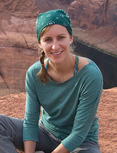
Hanka Uhlirova
ISI CAS, Brno
Scientist at complex photonics lab
Title
Multimode Fiber-Based Holographic Endomicroscopy: A Hair-Thin Path to Deep Brain Imaging in Animal Models
Abstract
We develop new endoscopes which are as narrow as human hair and provide extremely detailed observations anywhere in the living brain. Nowadays, they can routinely achieve monitoring of individual cells, resolve their connectivity and even record their activity within a neuronal circuit.
Bio
Hana Uhlířová is a senior scientist in the Complex Photonics group at ISI. She has a background in engineering and optics, with a strong focus on applying optical imaging technology to biological research. She has been interested in studying brain function, particularly the communication networks between different cell types and blood vessels involved in the brain's response to stimuli, known as the hemodynamic response. Currently, she is focused on using holographic endoscopes to achieve high-resolution imaging of neuronal circuits deep within the brain.
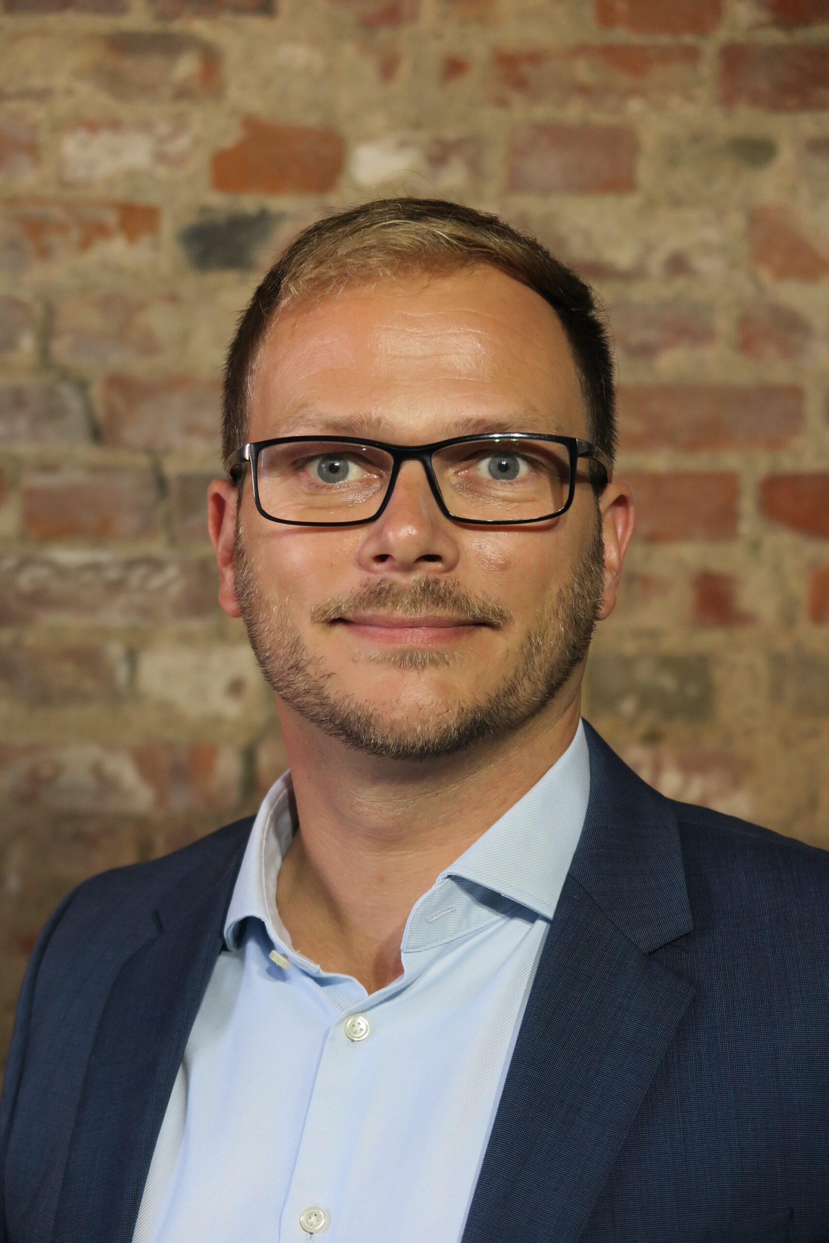
René Hammer
point electronic GmbH
Produktmanager
Title
Synchronized multi-channel multi-technique characterization in SEM and STEM
Abstract
A very wide range of material characterization techniques are used in Scanning Electron Microscopy (SEM) and Scanning Transmission Electron Microscopy (STEM). Standard microscopes generally provide detectors for the common imaging techniques, such as Secondary Electron (SE) detectors, Back-Scattered Electrons (BSE), Bright Field (BF) or High-Angle Angular Dark Field (HAADF). Additional characterization techniques are generally provided by third-party add-on systems, such as Energy Dispersive X-ray spectroscopy (EDS), Electron Beam Induced Current (EBIC), Cathodo-Luminescence (CL) and 4D STEM systems. Whilst add-on systems generally include synchronized characterization with standard detectors, synchronized imaging of all equipment required for correlative characterization remains challenging. We present here how advanced scan controllers can be employed to acquire multiple signals simultaneously, and, crucially, to synchronize multiple systems over digital trigger and synchronization signals.
Bio
Dr René Hammer graduated from Martin-Luther-University Halle-Wittenberg with a Physics diploma in 2007, and then continued in the Surface Science group as a PhD student and a Post Doc researcher to investigate structural and electronic structure of thin organic films on noble-metal single-crystals, which included low-temperature scanning-tunneling microscopy and spectroscopy. Dr. René Hammer joined point electronic GmbH in 2016, where he is currently a scientist and Product Manager for Electrical Analysis systems in SEM and TEM, focusing on instrument development and application science in a wide range of fields and industries, including semiconductor, energy and novel nano-devices.
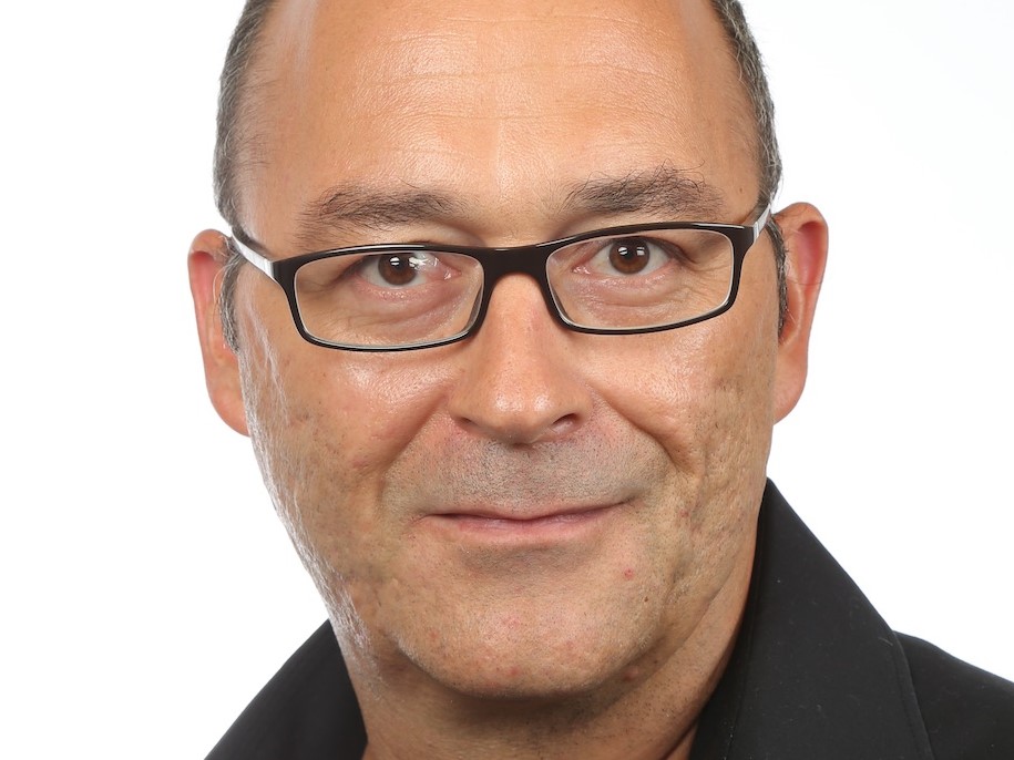
Marc Willinger
TU Munich
Leader of Electron Microscopy Group
Title
Observing while it happens: operando electron microscopy of non-equilibrium dynamics
Abstract
The relatively large chamber size of SEMs and the available space around the sample provide unique opportunities for combining complementary techniques for the simultaneous detection of diverse signals. Following the pioneering work of Gerry Danilatos [1], our group is developing environmental SEM for the study of gas phase and temperature induced processes such as material growth and decomposition or phase boundary dynamics and the emergence of catalytic function. Examples are used to highlight the importance of studying non-equilibrium states of matter.
[1] G.D. Danilatos “Foundations of Environmental Scanning Electron Microscopy”, Advances in Electronics and Electron Physics, Vol. 71, 1988, pp 109-250
Bio
Marc Willinger studied physics at the Technical University (TU) of Vienna and conducted his PhD studies at the Fritz Haber Institute (FHI) of the Max Planck Society. After a post-doc at the University of Aveiro in Portugal, he returned to the FHI as group leader for electron microscopy. There he started to develop and implement tools for multiscale operando electron microscopy. In 2018, he accepted a position as technical director at ScopeM, ETH Zurich. Since 2022 he is full professor at the TU Munich. He is interested in non-equilibrium states of matter, synergistic dynamics, and emergence of function.
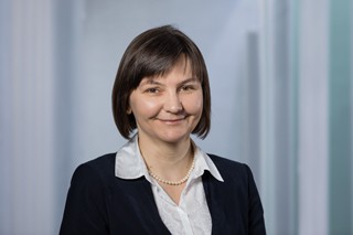
Malgorzata Kopycinska-Müller
Fraunhofer IKTS, Group ManagerCharacterization Technologies
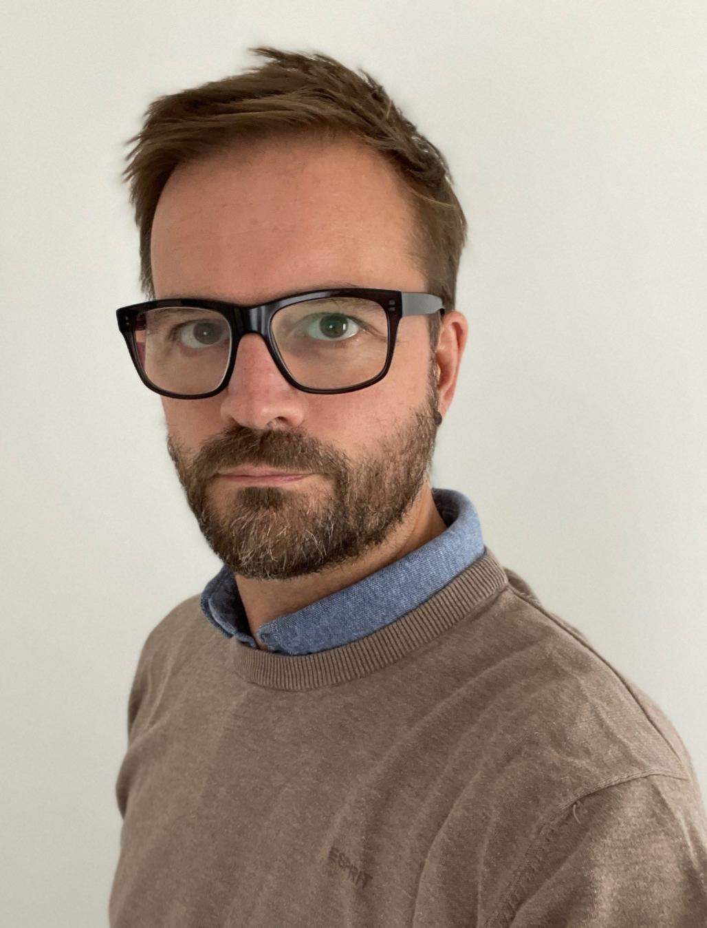
Andreas Meyer
Global Foundries
Dept. Director Analytical Labs GlobalFoundries Dresden
Title
Complex materials analysis in high-volume semiconductor manufacturing - case studies
Abstract
Technology development and high-volume manufacturing of semiconductor devices requires complex materials and failure analysis workflows to enable fast yield learning and troubleshooting. The combination of several lab-based analytical techniques with in-fab metrology techniques provides a powerful suite of tools for solving complex problems. The examples showcase these capabilities at GlobalFoundries.
Bio
Andreas Meyer studied Applied Physics at the University of Applied Sciences in Zwickau, Germany, where he received his first degree. He went on to study Instrumental Analytical Sciences at the Robert Gordon University in Aberdeen/Scotland receiving a Master of Science degree. In 2000 he joined the Analytical Labs department of AMDs Fab30 in Dresden, Germany. He started his career as Scanning Electron Microscopy engineer working on process development and failure analysis topics of Cu interconnects. During this time he worked on his PhD in the field of electromigration in Cu interconnect, which he received from Brandenburg University of Technology in Cottbus, Germany. Andreas Meyer is currently managing the Fab1 Analytical Labs department as site lead within the Global Analytical Labs organization of GlobalFoundries.
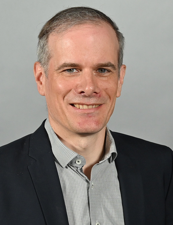
Holger Althus
Fraunhofer IWS Dresden
Division Manager Battery Materials
Title
Next-Gen Batteries: understanding storage mechanisms and degradation phenomena
Abstract
Solid-state batteries are expected to became a safe and high energy alternative to todays Lithium-Ion-Batteries. However, major challenges evolving around material compatibility, mechanical stress and interface instability between solid electrolyte and active materials need to be solved. Correlative characterization is required in order to improve the understanding on mechanisms of storage and degradation. Major research questions and preliminary structure/property correlations will be addressed by providing insights into current research results on solid state battery research.
Bio
Holger Althues studied chemical engineering and received his doctoral degree in inorganic chemistry at the University of Technology Dresden in 2007. Since then he is working at the Fraunhofer Institute for Material and Beam Technology in Dresden, Germany. 2008 he became a team manager for the chemical surface technology group and his team was transferred into a division in 2015. In his position as division manager he administrates various projects in the area of film deposition techniques, electrode processing and future generation batteries
Practical information

Panoramic view at the old town of Dresden, Germany. © Shutterstock
Dresden’s beauty is undisputed – and unmistakable it reveals itself to visitors at first glance and is characterized by one of the most beautiful historic city centers in Germany. At second glance, "Florence on the Elbe", as it is often called, attracts visitors with a wealth of art and culture on an international level. Locals and guests love and enjoy the city, its streets and squares and its concert halls with regular performances by world-class artists.
Moreover, Dresden is The City of Science in Germany. With 10 Fraunhofer institutes, 4 Max Planck institutes, 5 Leibnitz institutes, 2 Helmholtz institutes and Technische Universität Dresden as one of Germanys top ranked Universities of Excellence Dresden has the densest agglomeration of research institutions all over Europe. Dresden also ranks No. 1 in Europe with around 1,500 companies and 48,000 employees in the areas of information and communication technology and microelectronics. Therefore, the conference also serves a hub to discover new R&D opportunities in Europe.
We are looking forward to seeing you in Dresden.


